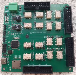
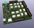
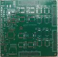
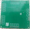
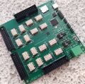
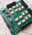
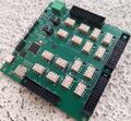
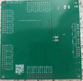
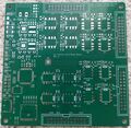
STM32 16 Channel Relay Board
This board was essentially designed as a prototype for a much larger product (64 channels).
The specifications were:
- Embedded STM32
- 16 Relays
- 2A per relay
Videos
The board have been covered in multiple videos. The first is covering the complete design after the board was ordered at JLCPCB but before the product had been received.
We did a quick (and bad) unboxing video when we received the board from JLCPCB:
Finally an in-depth test video:
Revision a
Design
Based on the specs the following details have been decided.
MCU
At first a STM32F103 was considered, but the "China market only" STM32F402 (which in reality is a STM32F401) is actually cheaper and quite a lot more powerful, so that one was chosen. Only nice to have feature which is not available in that is CAN.
Other
- Embedded STM32 (STM32F402)
- Dual buck converter - 5V and 3.3V
- 16 channels
- 2A per channel (2 x 1A)
- Built-in 16 MB Flash (W25Qxx)
- Micro-SD slot
Schematics
The overall board schematic will be like this:
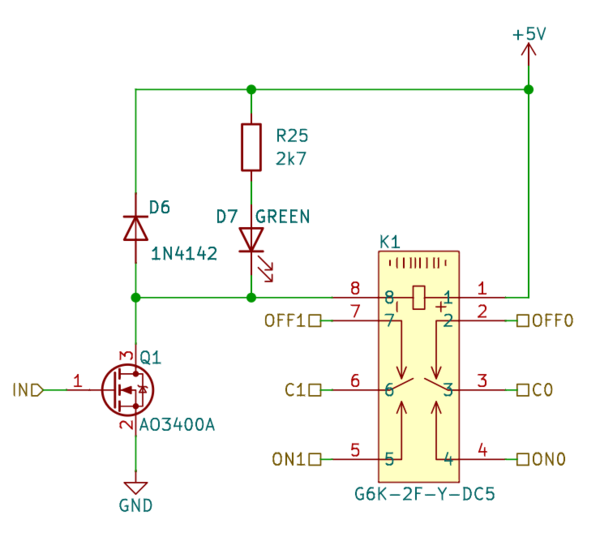
The relay channels are repeated 16 times:
The MOSFET is driven fully on with around 2V Vgs.
The Flyback Diode is primarily there to protect the LED and/or the MOSFET.
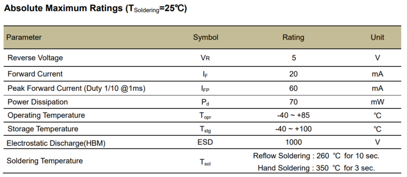
From the LED datasheet:
So, more than 5V reverse, and the LED will break down.
PCB
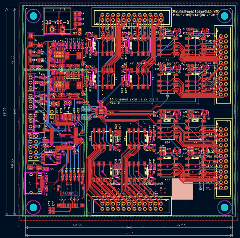
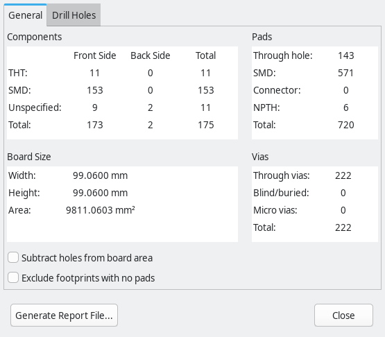
The PCB design was fairly trivial. JLCPCB got a slightly odd pricing model in small quantities where sizes up to 100x100 mm are really cheap but the price jump up after that, so the size of the board was deliberately chosen to be less than that. At the same time, some board edge was needed for the connectors.
While simple there are quite a lot of components.
Tests
The boards as received (see unboxing video) were thoroughly tested. The following sections go through all those tests.
| Test | Result | Remarks | ||
|---|---|---|---|---|
| Visual | Fail | Silk screen labeling the buttons are swapped BO/RST. | ||
| Default start bootloader. | Pass | [832522.603651] usb 3-10.5.4: new full-speed USB device number 114 using xhci_hcd [832522.692917] usb 3-10.5.4: New USB device found, idVendor=0483, idProduct=df11, bcdDevice=22.00 [832522.692923] usb 3-10.5.4: New USB device strings: Mfr=1, Product=2, SerialNumber=3 [832522.692925] usb 3-10.5.4: Product: STM32 BOOTLOADER [832522.692926] usb 3-10.5.4: Manufacturer: STMicroelectronics [832522.692928] usb 3-10.5.4: SerialNumber: 3578376E3233 | ||
| 3.3V supply on USB | Pass | Vbus measured 4.87V, Vin 4.47V, 3.3V rail = 3.4V | ||
| 5V supply on USB | Pass | Measured 5V = 4.3V [1] | ||
| 5V EN | Fail (Pass)[2] | When EN5V is driven it works as intended and the 5V can be controlled from the MCU. | ||
| SWD | Pass[3] | As expected, the Chinese market only STM32F402 show up as a STM32F401:
Found 1 stlink programmers version: V2J46S1 serial: 066DFF393056363043194823 flash: 262144 (pagesize: 16384) sram: 65536 chipid: 0x423 dev-type: STM32F401xB_xC | ||
| Boot0 | Pass | Holding down the B0 button while resetting or powering up will put the device into bootloader mode. | ||
| W25Q128 Flash | Pass | Working with LittleFS. Through LittleFS:
Writing 100 kB took 1719 ms Reading 100 kB took 223 ms Removing file took 165 ms | ||
| Micro-SD | Pass | Working as intended,
Testing Micro-SD FatFS ---- 4 /uptime.dat ---- 39 /tick.txt ---- 1048576 /big.dat Total blocks: 121528320 (60764 Mb) Free blocks : 101992192 (50996 Mb) Write 1 MB took 622 ms | ||
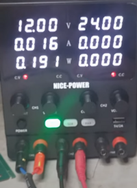
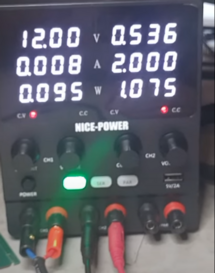
| Relays | Pass[4] | Board powered by left PSU at 12V. Right PSU set at 24V/2A[5]:
|
- ↑ With a Vin of 4.47V, 5V is obviously not achievable. However, for dev convenience it would be nice if it could deliver enough voltage to drive the relays. It basically ran as expected so let's call it an expected fail.
- ↑ By default and by mistake, EN was left floating. It needs to be driven hi for 5V PSU to go live.
- ↑ IF 3.3V is applied to the programming header, the MCU will be powered from that even if no USB or external power is connected, so the board can be flashed with just the programming header.
- ↑ This test as conducted probably make little sense. The resistance in the wires most likely exceed the resistance of the relay by an order of magnitude and the test would have to be executed hundreds of thousands of times to wear down the contacts in the relay. Yanking up the current to 5A would probably heat the cables up and the relay would most likely handle it fine.
- ↑ Notice! During this test the connection was to the off side, so one can actually see that the board consumption is higher when the load is high
Mystery fail
As this was a prototype and the component cost was on the high side (relays almost $1/each) I only had 2 boards assembled at JLCPCB. Of those 2 boards one was working flawlessly, the the 3.3V PSU on the second failed. No good reason for this failure have been found.
Revision b
Based on Revision a a few changes were made for Revision b. These changes can be summarized like this:
- 10 uH Coilcraft inductor changes to a much cheaper Chinese equivalent.
- Pull down on the EN5V signal so it is not left floating.
- Power rail test points changed to a 2 pin header.
Schematics
The overall board schematic will be like this:
The relay channels are repeated 16 times:
