PROTO
Jump to navigation
Jump to search
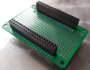
After producing the first few boards, the need for a quick prototyping board became obvious.
Schematic
PCB
The layout of the PCB becomes quite simple.
Example
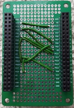
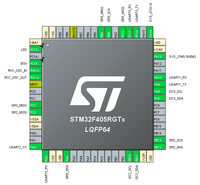
In this example we will be using the PROTO board to test uart, i2c and spi communication by creating the following connections:
| Peripheral | Signal | Pin | Pin | Signal | Peripheral | |
|---|---|---|---|---|---|---|
| Core | Boot0 | <--> | PC15 | GPIO | ||
| UART2 | TX | PA2 | <--> | PC11 | RX | UART3 |
| UART2 | RX | PA3 | <--> | PC10 | TX | UART3 |
| I2C2 | SCL | PB10 | <--> | PA8 | SCL | I2C3 |
| I2C2 | SDA | PB11 | <--> | PC9 | SDA | I2C3 |
| SPI2 | MOSI | PC3 | <--> | PC12 | MOSI | SPI3 |
| SPI2 | MISO | PC2 | <--> | PB4 | MISO | SPI3 |
| SPI2 | SCK | PB13 | <--> | PB3 | SCK | SPI3 |
| SPI2 | NSS | PB12 | <--> | PA4 | NSS | SPI3 |


