Almost as Simple as Possible (8-bit CPU)
About 6 years ago (at the time of writing), Ben Eater started a series of Youtube videos (see here, where he is building a very simple (but complete) 8 bit computer on a breadboard using almost exclusively discrete logic chips. Since then, this simple design has attracted a huge following and a lot of people have developed something similar. It has even gotten to a point where the original design has gotten itself a name - most people call it SAP-1 (Simple as Possible) although I don't think Ben Eater ever used that name himself.
I can not stress enough how big an inspiration those videos has been to me (and if you have not watched them, quit reading this page and go watch them now) and ever since watching them I have wanted to build one myself. However, I absolutely hate breadboards with a vengeance, so building SAP-1 on a breadboard was for me never a real option.
I was toying around with the idea of starting a series of PCB's putting the different modules together. This idea was/is attractive to me but the problem is that the old TTL/CMOS logic chips are getting quite expensive and some are hard to get.
Fortunately, a third option presented itself, when I got my hands on a ColorLight I5 module with accompanying extension board. With 25000 logic units, this FPGA is plenty big enough to implement something like this, and doing it in a FPGA will keep my desk way less messy than doing it on a breadboard.
Compared with Ben Eater's design, I made a few tentative decisions:
- All logic "active high"
- Ben Eater's design uses standard logic chips and these often use active low for signals like chip select and output enable. On a FPGA there's absolutely no reason to do this.
- 256 byte memory
- The original design had a shared program/memory space of 16 byte. This was done for a number of reasons but presumably mostly to cut down on the need of wires. Unfortunately 16 byte is ridiculously tight, so in this design we'll be expanding the address space to the full 8 bit = 256 byte.
Clock
The ColorLight I5 has got a 25 MHz crystal oscillator.
| Freq | Divider |
|---|---|
| 0.1 Hz | 125,000,000 |
| 1 Hz | 12,500,000 |
| 1 kHz | 12,500 |
| 1 MHz | 12 (ish) |
I/O Button and LED Board
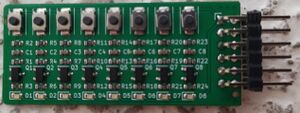
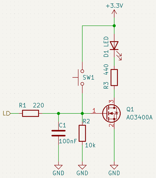
Monitoring all busses and registers would potentially require a lot of wires. To make that a bit easier, I created a small I/O board which hook up to 8 I/O pins. Each pin has got a LED driven by a MOSFET and also a button (in case it is input).
To test the boards themselves, as well as the I/O of the extension board, I hooked up 10 (which is the max as the remaining port is Ethernet). I ran a simple 8 bit counter on each and it looked like this:
It is worth noticing there are 2 issues. 2 bits are missing from the lower left port and 1 bit is hanging on the lower second from the left.
The missing 2 bits is because those are simply unconnected on the extension board (for some mysterious reason) and the hanging bit is because that pin is wired up to the STM32 MCU that is used to program the board.
All is well and I'll be able to monitor 8 8-bit ports in real time. The remaining can be used for input.
Block Diagram
The block diagram pretty much follow Ben Eater's original.
The main difference is that the memory address register is full 8 bit so that an entire 256 byte memory can be addressed.
Registers
The basic building block in our CPU is a register. All the registers (with one exception) are identical even if some registers in the design can only be written to (OUT and MAR).
In Verilog, the registers are implemented like this:
module register_module (
    input               rst,
    input               clk,
    input               ie,
    input               oe,
    output  reg [7:0]   data,
    inout       [7:0]   bus
);

    assign bus = (oe == 1'b1) ? data : 8'bzzzzzzzz;

    initial begin
        data = 8'd0;
    end

    always @ (negedge clk) begin

        if (rst == 1'b1) begin
            data = 8'd0;
        end else begin
            if (ie == 1'b1) begin
                 data = bus;
            end
        end

    end

endmodule
Gallery
Instruction set
| Mnemonic | Inst | Oper | Description |
|---|---|---|---|
| NOP | 0x00 | N/A | 1 byte instruction doing nothing (except increasing the program counter) |
| LDA | 0x01 | Address | Load RAM address into A |
| ADD | 0x02 | Address | Add value at address to A |
| SUB | 0x03 | Address | Subtract value at address from A |
| STA | 0x04 | Address | Store content of A to address |
| LDI | 0x05 | Immediate | Load value into A |
| JMP | 0x06 | Address | Unconditional jump to address |
| OUT | 0x07 | N/A | Copy A to OUT |
| CMP | 0x08 | Address | Compare value at address with value in A without modifying the A register |
| JZ | 0x09 | Address | Conditional jump if Zero flag is set (as a result of a CMP) |


