STM32 Readout Protection (RDP)
All STM32 MCUs feature something known as Readout Protection. It is probably a feature of the ARM Cortex core, since ST also provide something known as Proprietary Read Out Protection which is only available on certain STM32 models.
In this document we will take a brief look at the basic Read Out Protection of the MCU used on the Black Pill board, which is an STM32F411.
Readout Protection Levels
From the Reference Manual (pg. 53) the 3 different Read Out Protection levels are described as:
- Level 0: no read protection
- When the read protection level is set to Level 0 by writing 0xAA into the read protection option byte (RDP), all read/write operations (if no write protection is set) from/to the Flash memory are possible in all boot configurations (Flash user boot, debug or boot from RAM)
- Level 1: read protection enabled
- It is the default read protection level after option byte erase. The read protection Level 1 is activated by writing any value (except for 0xAA and 0xCC used to set Level 0 and Level 2, respectively) into the RDP option byte. When the read protection Level 1 is set:
- No access (read, erase, program) to Flash memory can be performed while the debug feature is connected or while booting from RAM or system memory bootloader. A bus error is generated in case of read request.
- When booting from Flash memory, accesses (read, erase, program) to Flash memory from user code are allowed.
- When Level 1 is active, programming the protection option byte (RDP) to Level 0 causes the Flash memory to be mass-erased. As a result the user code area is cleared before the read protection is removed. The mass erase only erases the user code area. The other option bytes including write protections remain unchanged from before the mass-erase operation. The OTP area is not affected by mass erase and remains unchanged. Mass erase is performed only when Level 1 is active and Level 0 requested. When the protection level is increased (0->1, 1->2, 0->2) there is no mass erase.
- It is the default read protection level after option byte erase. The read protection Level 1 is activated by writing any value (except for 0xAA and 0xCC used to set Level 0 and Level 2, respectively) into the RDP option byte. When the read protection Level 1 is set:
- Level 2: debug/chip read protection disabled
- The read protection Level 2 is activated by writing 0xCC to the RDP option byte. When the read protection Level 2 is set:
- All protections provided by Level 1 are active.
- Booting from RAM or system memory bootloader is no more allowed.
- JTAG, SWV (single-wire viewer), ETM, and boundary scan are disabled.
- User option bytes can no longer be changed.
- When booting from Flash memory, accesses (read, erase and program) to Flash memory from user code are allowed.
- Memory read protection Level 2 is an irreversible operation. When Level 2 is activated, the level of protection cannot be decreased to Level 0 or Level 1.
- The read protection Level 2 is activated by writing 0xCC to the RDP option byte. When the read protection Level 2 is set:
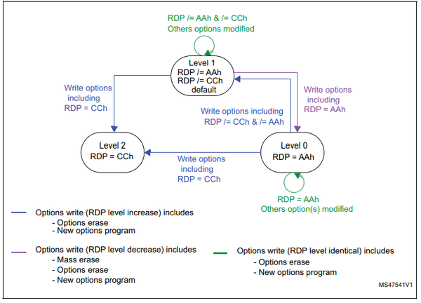
The most important thing to notice here is that Level 2 is irreversible while Level 1 can be reset at the loss of all Flash contents. This can be illustrated like this:
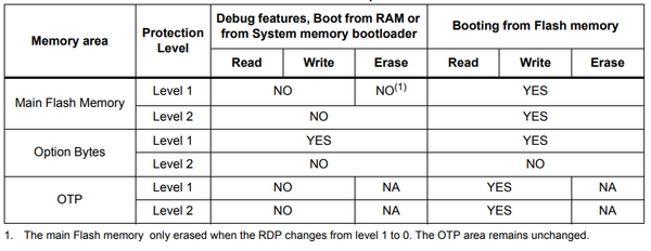
The actual protection level is described in the following table:
Test Example
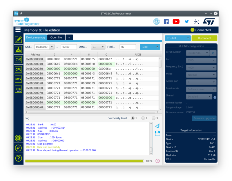
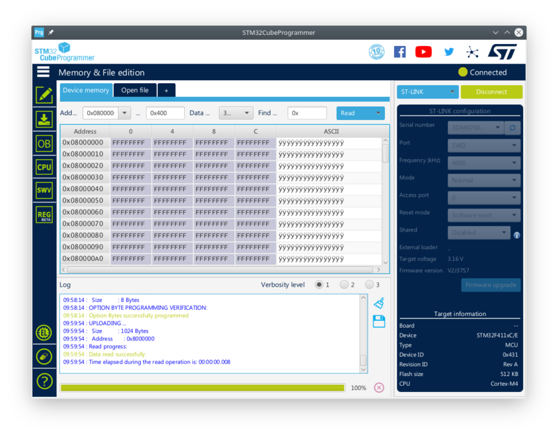
Using the STM32CubeProgrammer we can read out the code (flash) of a STM32 MCU (in this case a Black Pill board).
As can be seen, the internal flash content can be readily read out using the SWD.
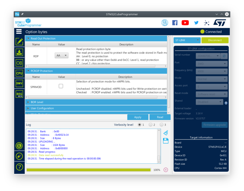
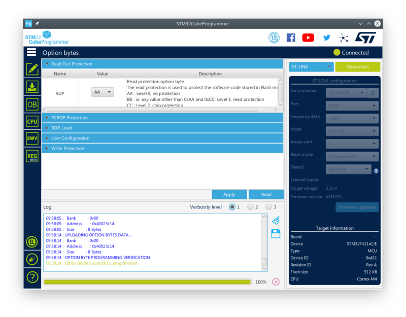
Switching to the Option Byte tab, the following is shown:
The RDP Open Byte contains "AA" which means Level 0 protection (or no protection at all).
We can now change the option byte to "BB" (Level 1 protection) and Apply the change.
Switching back to the Memory and File viewer we now get:
We can no longer read the content of the Internal flash.
At this point, attempting to flash the device result in an error:
st-flash 1.7.0-dirty
2021-07-04T09:56:00 INFO common.c: stm32f411re: 128 KiB SRAM, 4096 KiB flash in at least 16 KiB pages.
file blink.bin md5 checksum: 5fe5dd3e71839b5f8a08866109a59f3, stlink checksum: 0x002fe983
2021-07-04T09:56:00 INFO common.c: Attempting to write 31268 (0x7a24) bytes to stm32 address: 134250496 (0x8008000)
EraseFlash - Sector:0x2 Size:0x4000 2021-07-04T09:56:00 ERROR common.c: Flash memory is write protected
2021-07-04T09:56:00 ERROR common.c: Failed to erase_flash_page(0x8008000) == -1
stlink_fwrite_flash() == -1
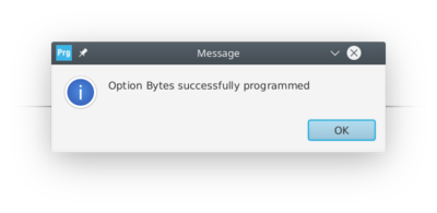
While Level 2 Read Out Protection is irreversible, the Level 1 Protection, which we activated, should be reversible, so going back to the Option Bytes tab we can attempt to change the value back to "AA" (Level 0). We notice that this time it takes a lot longer than before (5-10 seconds perhaps) but the result is the same:
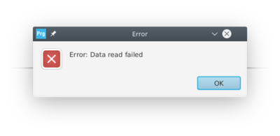
Trying to read out the flash contents now show:
In other words, as stated by ST Level 1 protection can be changed back to Level 0, but this result in a total loss of data.
