Difference between revisions of "Stm32Dev - rev. b (GD32F405 variant)"
| (5 intermediate revisions by the same user not shown) | |||
| Line 1: | Line 1: | ||
| − | [[Category:STM32]][[Category:STM32 Development Board]][[Category:STM32F405]][[Category:STM32 Hardware Development]]{{metadesc|Own design STM32 development board w. gd32f405 mcu}} | + | [[Category:STM32]][[Category:STM32 Hardware]][[Category:Development Board]][[Category:STM32 Development Board]][[Category:STM32F405]][[Category:STM32 Hardware Development]]{{metadesc|Own design STM32 development board w. gd32f405 mcu}} |
[[File:Stm32Dev rev. b - gd32f405 - top side unpopulated.jpg|thumb|STM32Dev rev. b gd32f405 version]] | [[File:Stm32Dev rev. b - gd32f405 - top side unpopulated.jpg|thumb|STM32Dev rev. b gd32f405 version]] | ||
To further test compatibility between stm32 and gd32 processors, I ordered a batch of [[Stm32Dev - rev. b|Stm32Dev]] boards with the [[STM32F405xx|STM32F405RGT6]] [[MCU]] replaced with a [[GD32F405xx|GD32F405RGT6]]. | To further test compatibility between stm32 and gd32 processors, I ordered a batch of [[Stm32Dev - rev. b|Stm32Dev]] boards with the [[STM32F405xx|STM32F405RGT6]] [[MCU]] replaced with a [[GD32F405xx|GD32F405RGT6]]. | ||
| − | To be absolutely certain that the boards were identical, the same gerbers were used, with only the bom modified (even down to the spelling mistake on the silk screen). | + | To be absolutely certain that the boards were identical, the same gerbers were used, with only the bom modified (even down to the spelling mistake on the silk screen). |
The point of this is to investigate if the GD32F4xx is drop in compatible with the STM32F4xx. | The point of this is to investigate if the GD32F4xx is drop in compatible with the STM32F4xx. | ||
| Line 29: | Line 29: | ||
{| | {| | ||
|- | |- | ||
| − | |[[File:Stm32Dev rev. b - top side unpopulated.jpg|500px | + | |[[File:Stm32Dev rev. b - top side unpopulated.jpg|500px]] |
|[[File:Stm32Dev rev. b - unpopulated.jpg|500px]] | |[[File:Stm32Dev rev. b - unpopulated.jpg|500px]] | ||
| + | |- | ||
| + | |Original w. stm32f405 - top | ||
| + | |Original w. typo on silk - bottom | ||
|- | |- | ||
|[[File:Stm32Dev rev. b - gd32f405 - top side unpopulated.jpg|500px]] | |[[File:Stm32Dev rev. b - gd32f405 - top side unpopulated.jpg|500px]] | ||
|[[File:Stm32Dev rev. b - gd32f405 - unpopulated.jpg|500px]] | |[[File:Stm32Dev rev. b - gd32f405 - unpopulated.jpg|500px]] | ||
| + | |- | ||
| + | |Black soldermask and gd32f405 - top | ||
| + | |Black soldermask - identical typo - bottom | ||
|} | |} | ||
Revision as of 09:07, 27 October 2021
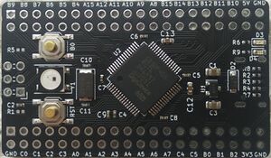
To further test compatibility between stm32 and gd32 processors, I ordered a batch of Stm32Dev boards with the STM32F405RGT6 MCU replaced with a GD32F405RGT6.
To be absolutely certain that the boards were identical, the same gerbers were used, with only the bom modified (even down to the spelling mistake on the silk screen).
The point of this is to investigate if the GD32F4xx is drop in compatible with the STM32F4xx.
Flashing
To do a command line flash, I usually use the st-flash command.
DFU
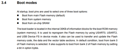
It is a little unclear if DFU is supported.
There is no mention of DFU in any of the manuals, but in the datasheet the following is stated:
However, in the user manual it says:
The device refuse to show up as a DFU device, so I'll assume DFU is not supported.
Physical Device
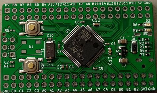
|
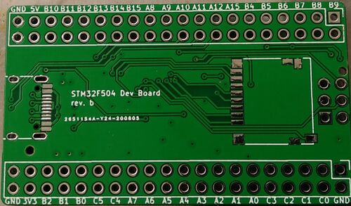
|
| Original w. stm32f405 - top | Original w. typo on silk - bottom |
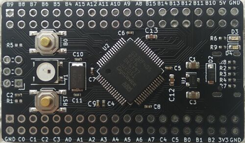
|
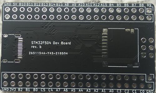
|
| Black soldermask and gd32f405 - top | Black soldermask - identical typo - bottom |
Timer Interrupt
Simple test if the timers - including timer interrupt - is running as expected.
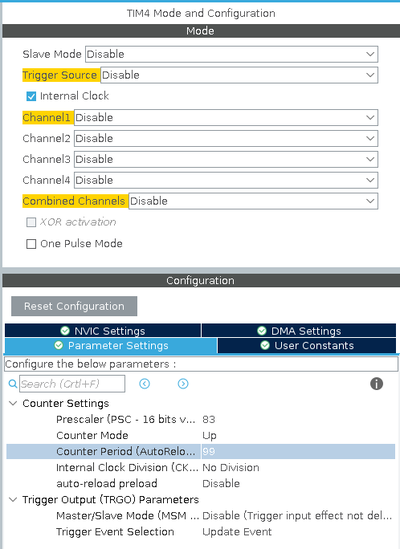
Configured TIM4 as follows:
Created a simple call back:
/* USER CODE BEGIN 0 */
// Override the weak call back function
void HAL_TIM_PeriodElapsedCallback(TIM_HandleTypeDef *htim) {
      if (htim->Instance == TIM4) {
              HAL_GPIO_TogglePin(CLK_GPIO_Port, CLK_Pin);
      }
}
/* USER CODE END 0 */
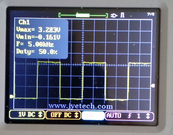
The APB1 timer clock is 84 MHz, so in theory this should result in a 5 KHz clock on the CLK pin.
Which is spot on as expected. This also mean that the clock configuration is acceptable (configured with 8 MHz external oscillator and 168 MHz CPU clock resulting in the 84 MHz APB1 timer clock).
DACs (and DMA)
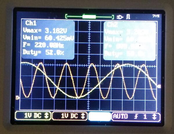
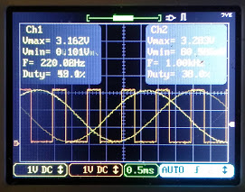
Another test that was easy for me to run was a test of the DACs driven by DMA. I already had an application which was running two audio oscillators (48 kHz sample rate - see STM32 Audio Analogue ADC and DAC using Timer + DMA). The result was again promising:
A bonus of this particular application is that it uses the CMSIS DSP library to do the sine wave calculation. In the firmware it looks like:
	for (uint8_t sample = 0; sample < BUFFER_SIZE; sample++) {

		*dac1_buffer_ptr = (uint16_t) (DAC_MID
				+ osc1_amp * arm_sin_f32(osc1_angle) * DAC_MID);
		*dac2_buffer_ptr = (uint16_t) (DAC_MID
				+ osc2_amp * arm_sin_f32(osc2_angle) * DAC_MID);
		osc1_angle += osc1_angle_per_sample;
		osc2_angle += osc2_angle_per_sample;
		dac1_buffer_ptr++;
		dac2_buffer_ptr++;

		if (osc1_angle > M_PI2)
			osc1_angle -= M_PI2;
		if (osc2_angle > M_PI2)
			osc2_angle -= M_PI2;

	}
In other words, it uses the arm_sin_f32 (from the CMSIS DSP library) to calculate the sine wave. The application is running at 48 kHz sample rate with a DMA buffer of 48 samples. In other word, the calculation is performed once per ms per channel (so twice) calculating the value of 48 * 2 samples in total. Timing wise, that looks like this:
It spends roughly 0.2 ms every ms to calculate the samples for the DACs.
