Difference between revisions of "STM32 SD"
Jump to navigation
Jump to search
| Line 2: | Line 2: | ||
{| width=100% | {| width=100% | ||
|- | |- | ||
| − | | width= | + | | width=85% valign=top | |
{| class="wikitable sortable" width=100% | {| class="wikitable sortable" width=100% | ||
|- | |- | ||
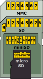
! Name | ! Name | ||
! Pin on SD | ! Pin on SD | ||
| − | ! | + | ! F411 |
| + | ! F405 | ||
! Description | ! Description | ||
|- | |- | ||
| Line 13: | Line 14: | ||
| 1 | | 1 | ||
| PA8 | | PA8 | ||
| + | | | ||
| Serial Data 3 | | Serial Data 3 | ||
|- | |- | ||
| Line 23: | Line 25: | ||
| 3 | | 3 | ||
| N/C | | N/C | ||
| + | | | ||
| Not connected/used on micro-SD | | Not connected/used on micro-SD | ||
|- | |- | ||
| Line 28: | Line 31: | ||
| 4 | | 4 | ||
| 3.3V | | 3.3V | ||
| + | | | ||
| Power supply | | Power supply | ||
|- | |- | ||
| Line 33: | Line 37: | ||
| 5 | | 5 | ||
| PB15 | | PB15 | ||
| + | | | ||
| Clock | | Clock | ||
|- | |- | ||
| Line 38: | Line 43: | ||
| 6 | | 6 | ||
| GND | | GND | ||
| + | | | ||
| Ground | | Ground | ||
|- | |- | ||
| Line 43: | Line 49: | ||
| 7 | | 7 | ||
| PB4 | | PB4 | ||
| + | | | ||
| Serial Data 0 | | Serial Data 0 | ||
|- | |- | ||
| Line 48: | Line 55: | ||
| 8 | | 8 | ||
| PA8 | | PA8 | ||
| + | | | ||
| Serial Data 1 | | Serial Data 1 | ||
|- | |- | ||
| Line 53: | Line 61: | ||
| 9 | | 9 | ||
| PA9 | | PA9 | ||
| + | | | ||
| Serial Data 2 | | Serial Data 2 | ||
|} | |} | ||
Revision as of 03:35, 12 January 2021
Black Pill
| Name | Pin on SD | STM32F411 |
|---|---|---|
| DAT3 | 1 | PA8 |
