Difference between revisions of "STM32 Bit Banding (or bit-banding)"
| Line 11: | Line 11: | ||
[[File:Bit Band Formula.png|600px]] | [[File:Bit Band Formula.png|600px]] | ||
</div> | </div> | ||
| + | |||
| + | The values are defined in the 'stm32f405xx.h' file generated by [[STM32CubeMX]]: | ||
<pre> | <pre> | ||
| − | #define | + | #define FLASH_BASE 0x08000000UL /*!< FLASH(up to 1 MB) base address in the alias region */ |
| − | #define | + | #define CCMDATARAM_BASE 0x10000000UL /*!< CCM(core coupled memory) data RAM(64 KB) base address in the alias region */ |
| − | #define | + | #define SRAM1_BASE 0x20000000UL /*!< SRAM1(112 KB) base address in the alias region */ |
| − | #define | + | #define SRAM2_BASE 0x2001C000UL /*!< SRAM2(16 KB) base address in the alias region */ |
| + | #define PERIPH_BASE 0x40000000UL /*!< Peripheral base address in the alias region */ | ||
| + | #define BKPSRAM_BASE 0x40024000UL /*!< Backup SRAM(4 KB) base address in the alias region */ | ||
| + | #define FSMC_R_BASE 0xA0000000UL /*!< FSMC registers base address */ | ||
| + | #define SRAM1_BB_BASE 0x22000000UL /*!< SRAM1(112 KB) base address in the bit-band region */ | ||
| + | #define SRAM2_BB_BASE 0x22380000UL /*!< SRAM2(16 KB) base address in the bit-band region */ | ||
| + | #define PERIPH_BB_BASE 0x42000000UL /*!< Peripheral base address in the bit-band region */ | ||
| + | #define BKPSRAM_BB_BASE 0x42480000UL /*!< Backup SRAM(4 KB) base address in the bit-band region */ | ||
| + | #define FLASH_END 0x080FFFFFUL /*!< FLASH end address */ | ||
| + | #define FLASH_OTP_BASE 0x1FFF7800UL /*!< Base address of : (up to 528 Bytes) embedded FLASH OTP Area */ | ||
| + | #define FLASH_OTP_END 0x1FFF7A0FUL /*!< End address of : (up to 528 Bytes) embedded FLASH OTP Area */ | ||
| + | #define CCMDATARAM_END 0x1000FFFFUL /*!< CCM data RAM end address | ||
| + | </pre> | ||
| + | Using the formula, we can now create some macros to calculate the bit band address for both SRAM and peripherals: | ||
| + | |||
| + | <pre> | ||
#define bitband_t *(volatile uint32_t*) | #define bitband_t *(volatile uint32_t*) | ||
| − | #define m_BITBAND_SRAM(address,bit) ( | + | #define m_BITBAND_SRAM(address,bit) (SRAM1_BB_BASE + (((uint32_t)address) - SRAM1_BASE) * 32 + (bit) * 4) |
| − | #define m_BITBAND_PERIPH(address,bit) ( | + | #define m_BITBAND_PERIPH(address,bit) (PERIPH_BB_BASE + (((uint32_t)address) - PERIPH_BASE) * 32 + (bit) * 4) |
</pre> | </pre> | ||
Revision as of 03:30, 21 October 2024
In older 8-bit MCUs it was quite common to have instructions to clear or set a bit as one atomic instruction. By atomic it means the read->modify->write can not be interrupted resulting in other bits being set wrongly. Unfortunately ARM did not implement such instructions in the ARM cores. They did however implement something known as "bit banding" (or bit-banding).
Bit banding is an aliased region of memory addresses where each address point to exactly one bit in the original byte. These bytes get updated accordingly to the bits in the original byte and when or if changes only that single bit of the original get set or reset. There are two of these bands. One is covering the entire SRAM space and one is covering all the peripheral registers.
Calculating Bit Band Address
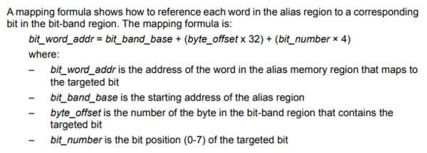
The formula for calculating the bit band address is described in the reference manual (for the STM32F405 here) like this:
The values are defined in the 'stm32f405xx.h' file generated by STM32CubeMX:
#define FLASH_BASE            0x08000000UL /*!< FLASH(up to 1 MB) base address in the alias region                         */
#define CCMDATARAM_BASE       0x10000000UL /*!< CCM(core coupled memory) data RAM(64 KB) base address in the alias region  */
#define SRAM1_BASE            0x20000000UL /*!< SRAM1(112 KB) base address in the alias region                              */
#define SRAM2_BASE            0x2001C000UL /*!< SRAM2(16 KB) base address in the alias region                              */
#define PERIPH_BASE           0x40000000UL /*!< Peripheral base address in the alias region                                */
#define BKPSRAM_BASE          0x40024000UL /*!< Backup SRAM(4 KB) base address in the alias region                         */
#define FSMC_R_BASE           0xA0000000UL /*!< FSMC registers base address                                                */
#define SRAM1_BB_BASE         0x22000000UL /*!< SRAM1(112 KB) base address in the bit-band region                          */
#define SRAM2_BB_BASE         0x22380000UL /*!< SRAM2(16 KB) base address in the bit-band region                           */
#define PERIPH_BB_BASE        0x42000000UL /*!< Peripheral base address in the bit-band region                             */
#define BKPSRAM_BB_BASE       0x42480000UL /*!< Backup SRAM(4 KB) base address in the bit-band region                      */
#define FLASH_END             0x080FFFFFUL /*!< FLASH end address                                                          */
#define FLASH_OTP_BASE        0x1FFF7800UL /*!< Base address of : (up to 528 Bytes) embedded FLASH OTP Area                */
#define FLASH_OTP_END         0x1FFF7A0FUL /*!< End address of : (up to 528 Bytes) embedded FLASH OTP Area                 */
#define CCMDATARAM_END        0x1000FFFFUL /*!< CCM data RAM end address
Using the formula, we can now create some macros to calculate the bit band address for both SRAM and peripherals:
#define bitband_t *(volatile uint32_t*)

#define m_BITBAND_SRAM(address,bit) (SRAM1_BB_BASE + (((uint32_t)address) - SRAM1_BASE) * 32 + (bit) * 4)
#define m_BITBAND_PERIPH(address,bit) (PERIPH_BB_BASE + (((uint32_t)address) - PERIPH_BASE) * 32 + (bit) * 4)
Usage Examples
Considering a variable v, the bits can be individually set/reset like this:
*((uint8_t *)m_BITBAND_SRAM(&v, 7)) = 1;
*((uint8_t *)m_BITBAND_SRAM(&v, 6)) = 0;
*((uint8_t *)m_BITBAND_SRAM(&v, 5)) = 1;
*((uint8_t *)m_BITBAND_SRAM(&v, 4)) = 0;
*((uint8_t *)m_BITBAND_SRAM(&v, 3)) = 1;
*((uint8_t *)m_BITBAND_SRAM(&v, 2)) = 0;
*((uint8_t *)m_BITBAND_SRAM(&v, 1)) = 1;
*((uint8_t *)m_BITBAND_SRAM(&v, 0)) = 0;
A peripheral - for example port 13 on GPIOC can be handled like this:
uint8_t *led_pin = (uint8_t *)m_BITBAND_PERIPH(&LED_GPIO_Port->ODR, 13);

// Toggle LED
*led_pin = !*led_pin;
Miscellaneous Links
To be added
