Difference between revisions of "Serial Flash - W25Qxxx QuadSPI"
Jump to navigation
Jump to search
| Line 137: | Line 137: | ||
* [https://datasheet.lcsc.com/szlcsc/Winbond-Elec-W25Q128JVSIQTR_C97521.pdf W25Q128JV Datasheet] | * [https://datasheet.lcsc.com/szlcsc/Winbond-Elec-W25Q128JVSIQTR_C97521.pdf W25Q128JV Datasheet] | ||
| + | * [https://datasheet.lcsc.com/lcsc/2106062244_GigaDevice-Semicon-Beijing-GD25Q128ESIG_C2758105.pdf GD25Q128E Datasheet] | ||
* [https://datasheet.lcsc.com/lcsc/1912111437_GigaDevice-Semicon-Beijing-GD25LQ64CSIGR_C395493.pdf GD25LQ64C Datasheet] | * [https://datasheet.lcsc.com/lcsc/1912111437_GigaDevice-Semicon-Beijing-GD25LQ64CSIGR_C395493.pdf GD25LQ64C Datasheet] | ||
* [https://www.programmersought.com/article/39481457418/ LittleFS on SPI Flash (W28Q64)] | * [https://www.programmersought.com/article/39481457418/ LittleFS on SPI Flash (W28Q64)] | ||
Revision as of 01:21, 29 June 2021
Serial flash IC's are quite common. They are typically named M25Qxxx where M is the manufacturer (W is for Winbond) and xxx is the size in bits. So the "W25Q128JV" is a Winbond flash with 128 bits = 16 MB.
Pinout
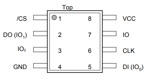
The serial flash IC's typically have a pinout like:
They can operate in either plain SPI mode (using DI and DO as MOSI/MISO) or so-called Quad SPI (4 data lines) using IO0-IO3.
Memory Organisation
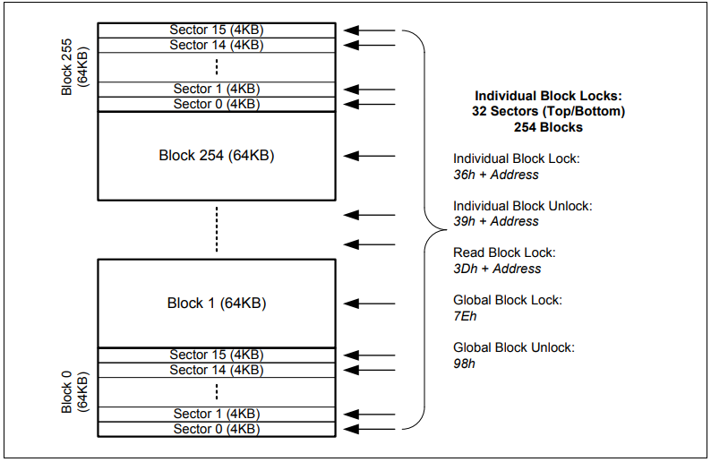
Internally the flash is organised like this:
Bytes in the flash can be read/write individually, but before "writing" the address of the write needs to be "erased" (set to 0xff) and erase can only be done by "sector" (4kB in the above example -
STM32L4 training - Hands-on QSPI
Source Example
Working:
	QSPI_CommandTypeDef sCommand;
	static uint8_t id[17] = { 0 };
	static uint8_t tx_buf[0x10] = "Ext Flash";
	static uint8_t rx_buf[0x10] = { 0 };

	sCommand.DdrMode = QSPI_DDR_MODE_DISABLE;
	sCommand.DdrHoldHalfCycle = QSPI_DDR_HHC_ANALOG_DELAY;
	sCommand.SIOOMode = QSPI_SIOO_INST_EVERY_CMD;

	/***** Read ID operation*****/
	sCommand.Instruction = 0x9F; //READ ID command code
	sCommand.InstructionMode = QSPI_INSTRUCTION_1_LINE; //Command line width
	sCommand.AddressMode = QSPI_ADDRESS_NONE; //Address line width. No address phase
	sCommand.DataMode = QSPI_DATA_1_LINE; //Data line width
	sCommand.NbData = 17; //Read the data length. ID length is 17 bytes
	sCommand.AlternateByteMode = QSPI_ALTERNATE_BYTES_NONE; //No multiplexing byte stage
	sCommand.DummyCycles = 0; //No Dummy phase
	//Configuration command (when there is data stage, the command will be sent in the subsequent sending/receiving API call)
	if (HAL_QSPI_Command(&hqspi, &sCommand, 5000) != HAL_OK) {
		Error_Handler();
	}
	//Execute QSPI reception
	if (HAL_QSPI_Receive(&hqspi, id, 5000) != HAL_OK) {
		Error_Handler();
	}

	/***** Write enable operation (need to make the external memory in the write enable state before block erasing) *****/
	sCommand.Instruction = 0x06; //Write enable command code
	sCommand.InstructionMode = QSPI_INSTRUCTION_1_LINE; //Command line width
	sCommand.AddressMode = QSPI_ADDRESS_NONE; //Address line width. No address phase
	sCommand.DataMode = QSPI_DATA_NONE; //Data line width. No data stage
	sCommand.AlternateByteMode = QSPI_ALTERNATE_BYTES_NONE; //No multiplexing byte stage
	sCommand.DummyCycles = 0; //No Dummy phase
	//Configure sending command
	if (HAL_QSPI_Command(&hqspi, &sCommand, 5000) != HAL_OK) {
		Error_Handler();
	}

	/***** Block erase operation*****/
	sCommand.Instruction = 0xD8; //Sector erase command code
	sCommand.InstructionMode = QSPI_INSTRUCTION_1_LINE; //Command line width
	sCommand.AddressMode = QSPI_ADDRESS_1_LINE; //Address line width. No address phase
	sCommand.AddressSize = QSPI_ADDRESS_24_BITS; //Address length
	sCommand.Address = 0; //Any address in the sector to be erased.
	sCommand.DataMode = QSPI_DATA_NONE; //Data line width. No data stage
	sCommand.AlternateByteMode = QSPI_ALTERNATE_BYTES_NONE; //No multiplexing byte stage
	sCommand.DummyCycles = 0; //No Dummy phase
	//Configure sending command
	if (HAL_QSPI_Command(&hqspi, &sCommand, 5000) != HAL_OK) {
		Error_Handler();
	}
	HAL_Delay(3000); //Delay 3s. The unit is SysTick timer interrupt period

	/***** Write enable operation (need to make the external memory in the write enable state before block erasing) *****/
	sCommand.Instruction = 0x06; //Write enable command code
	sCommand.InstructionMode = QSPI_INSTRUCTION_1_LINE; //Command line width
	sCommand.AddressMode = QSPI_ADDRESS_NONE; //Address line width. No address phase
	sCommand.DataMode = QSPI_DATA_NONE; //Data line width. No data stage
	sCommand.AlternateByteMode = QSPI_ALTERNATE_BYTES_NONE; //No multiplexing byte stage
	sCommand.DummyCycles = 0; //No Dummy phase
	//Configure sending command
	if (HAL_QSPI_Command(&hqspi, &sCommand, 5000) != HAL_OK) {
		Error_Handler();
	}

	/***** Four-wire fast write operation*****/
	sCommand.Instruction = 0x32; //Quick write command code with four lines
	sCommand.InstructionMode = QSPI_INSTRUCTION_1_LINE; //Command line width
	sCommand.AddressMode = QSPI_ADDRESS_1_LINE; //Address line width
	sCommand.AddressSize = QSPI_ADDRESS_24_BITS; //Address length
	sCommand.Address = 0; //Write the starting address
	sCommand.DataMode = QSPI_DATA_4_LINES; //Data line width
	sCommand.NbData = 10; //write data length
	sCommand.AlternateByteMode = QSPI_ALTERNATE_BYTES_NONE; //No multiplexing byte stage
	sCommand.DummyCycles = 0; //No Dummy phase
	//Configuration command (when there is data stage, the command will be sent in the subsequent sending/receiving API call)
	if (HAL_QSPI_Command(&hqspi, &sCommand, 5000) != HAL_OK) {
		Error_Handler();
	}
	//Execute QSPI reception
	if (HAL_QSPI_Transmit(&hqspi, tx_buf, 5000) != HAL_OK) {
		Error_Handler();
	}
	HAL_Delay(5); //Delay 5ms. The unit is SysTick timer interrupt period

	/***** Four-wire fast read operation*****/
	sCommand.Instruction = 0x6B; //Quick read command code with four lines
	sCommand.InstructionMode = QSPI_INSTRUCTION_1_LINE; //Command line width
	sCommand.AddressMode = QSPI_ADDRESS_1_LINE; //Address line width
	sCommand.AddressSize = QSPI_ADDRESS_24_BITS; //Address length
	sCommand.Address = 0; //Start address
	sCommand.DataMode = QSPI_DATA_4_LINES; //Data line width
	sCommand.NbData = 10; //Read data length
	sCommand.AlternateByteMode = QSPI_ALTERNATE_BYTES_NONE; //No multiplexing byte stage
	sCommand.DummyCycles = 8; //Dummy phase. N25Q128A13EF840F

	//Configuration command (when there is data stage, the command will be sent in the subsequent sending/receiving API call)
	if (HAL_QSPI_Command(&hqspi, &sCommand, 5000) != HAL_OK) {
		Error_Handler();
	}
	//Execute QSPI reception
	if (HAL_QSPI_Receive(&hqspi, rx_buf, 5000) != HAL_OK) {
		Error_Handler();
	}

