Difference between revisions of "ST-Link"
| Line 27: | Line 27: | ||
PC13 and PC14 (and possibly PC15 in the future) appears to be working as a means for the firmware to identify the "version" of the hardware. On above schematics, PC13 is pulled low with a resistor while PC14 (and PC15) are left floating. | PC13 and PC14 (and possibly PC15 in the future) appears to be working as a means for the firmware to identify the "version" of the hardware. On above schematics, PC13 is pulled low with a resistor while PC14 (and PC15) are left floating. | ||
| + | |||
| + | A voltage divider splitting +3.3 V in half is connected to PA0 and labelled AIN_1. The ST-Link devices are capable of measuring the target processor supply voltage and this is probably a workaround of the development boards (which know their supply voltage already). | ||
| + | |||
| + | The "output" pins of the ST-Link V2 are as follows: | ||
| + | |||
| + | {| | ||
| + | |- | ||
| + | | Pin | ||
| + | | Label | ||
| + | | Remarks | ||
| + | |} | ||
Revision as of 03:39, 28 November 2020
There's a number of different ways to flash STM32 devices. One of these is to use ST's own ST-Link devices.
There are multiple benefits of using one of these ST-Link devices rather than a plain serial dongle:
- The device need not be restarted in flash mode (Boot0)
- Programs can be debugged on the device
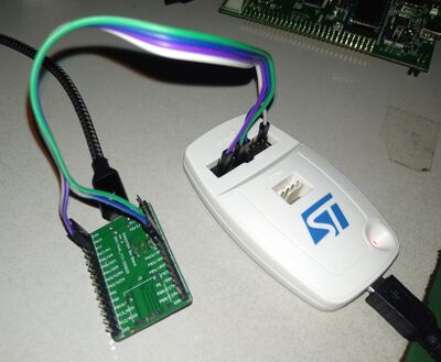
The official ST-Link as seen above are relatively cheap (< $20) and there are Chinese copies available (haven't tried those).
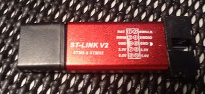
The most common option are these:
They are Chinese knock offs and they run the official ST-Link firmware.
Hardware Analysis
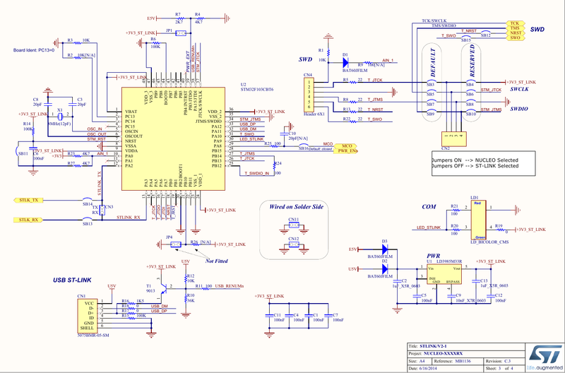
ST does not make schematics or source code available for the official ST-Link devices, which is a pity (and a someone odd business decision). However, they do publish a partial schematics since a built-in ST-Link device is included in all their development boards, a partial schematics is available.
From the schematics we can see that the ST-Link device is build around a STM32F103CBT6 which is the 128 kB Flash version.
PC13 and PC14 (and possibly PC15 in the future) appears to be working as a means for the firmware to identify the "version" of the hardware. On above schematics, PC13 is pulled low with a resistor while PC14 (and PC15) are left floating.
A voltage divider splitting +3.3 V in half is connected to PA0 and labelled AIN_1. The ST-Link devices are capable of measuring the target processor supply voltage and this is probably a workaround of the development boards (which know their supply voltage already).
The "output" pins of the ST-Link V2 are as follows:
| Pin | Label | Remarks |


