Difference between revisions of "DIY STM32 Programmer (ST-Link/V2-1)"
| Line 48: | Line 48: | ||
[[User:Lth|I]] think what is going on there is ensuring the D+ is pulled high through the 1.5 kOhm resistor unless the RENUM signal is forced low. The voltage divider R4/R5 and R6 are merely there to protect the transistor itself. While I do understand what they ([[ST]]) are trying to achieve, I would say they could have achieved this much simpler. IF the D+ was simply permanently pulled high by the 1.5 kOhm resistor, since it is connected to a GPIO pin, this GPIO pin could simply be briefly yanked low at MCU reset. | [[User:Lth|I]] think what is going on there is ensuring the D+ is pulled high through the 1.5 kOhm resistor unless the RENUM signal is forced low. The voltage divider R4/R5 and R6 are merely there to protect the transistor itself. While I do understand what they ([[ST]]) are trying to achieve, I would say they could have achieved this much simpler. IF the D+ was simply permanently pulled high by the 1.5 kOhm resistor, since it is connected to a GPIO pin, this GPIO pin could simply be briefly yanked low at MCU reset. | ||
| − | As for [[MCU]] the original [[ST-Link/V2-1]] uses an [[STM32F103|STM32F103CB]] (128 kB flash). | + | As for [[MCU]] the original [[ST-Link/V2-1]] uses an [[STM32F103|STM32F103CB]] (128 kB flash). Since it is well known that STM32F103C8 [[MCU]]s also have 128 kB flash this one should do nicely too. In this case however, due to the general shortage of [[STM32]] [[MCU]]s, I went with a [[GigaDevice]] [[GD32]] instead. |
== PCB == | == PCB == | ||
Revision as of 04:44, 22 July 2021
ST-Link devices are almost essential when developing software for the STM32 MCUs. They are relatively cheap and easily available.
They roughly fall into two different categories. ST themselves make a number of them and they all work quite well.
One thing that annoys me with the original ST-Link devices is that the programming header is unlabelled. This essentially mean that every time I use it I have to Google for the actual pinout.
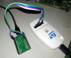
Also, the ones I've got (the one in the photo to the right) are ST-Link/V2 devices.
Before diving into any further details, credits to Martin from EmbeddedBlog who went through the same as here. His project is linked under Miscellaneous Links.
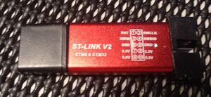
There are also a lot of Chinese clones available and while they have some limitations they also work quite well.
Unfortunately these devices are also ST-Link/V2 devices, and they do not have the SWO pin on the header, so any debug trace is impossible. For flashing and normal debugging they work fine though.
In short, the ST-Link/V2.1 devices offer a few extra features:
- Serial Wire Trace (SWO)
- Virtual serial port
- Mass storage
All features that, while not absolutely essential, does come quite handy.
Another reason for creating my own "programmer" is that I can experiment with using a GigaDevice GD32F103, which are much easier to source at the moment.
Original ST-Link V2.1
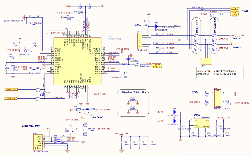
The schematic of the original ST-Link is readily available from the various Nucleo development modules.
A bit messy schematics but it'll do.
Schematics
Based on ST's original schematics, creating a version using only parts from JLCPCB's parts library was easy (and much nicer if I shall say so myself).
One thing I left out was the serial resistors of the programming header. This might very well come back and bite me in the ass but space is going to be at a premium.
The main difference hardware wise between ST-Link/V2 and ST-Link/V2-1 is the renumeration circuitry:
I think what is going on there is ensuring the D+ is pulled high through the 1.5 kOhm resistor unless the RENUM signal is forced low. The voltage divider R4/R5 and R6 are merely there to protect the transistor itself. While I do understand what they (ST) are trying to achieve, I would say they could have achieved this much simpler. IF the D+ was simply permanently pulled high by the 1.5 kOhm resistor, since it is connected to a GPIO pin, this GPIO pin could simply be briefly yanked low at MCU reset.
As for MCU the original ST-Link/V2-1 uses an STM32F103CB (128 kB flash). Since it is well known that STM32F103C8 MCUs also have 128 kB flash this one should do nicely too. In this case however, due to the general shortage of STM32 MCUs, I went with a GigaDevice GD32 instead.
PCB
For hobby projects like this I will usually stick with double-sided PCB. But in this particular case I wanted this to fit into the aluminium "sleeve" of the Chinese knock off ST-Link devices, so space was at a premium. Also, pricing wise there's not much difference these days, so I went for a four layer PCB and kept +3.3V and GND on the two inner layers.
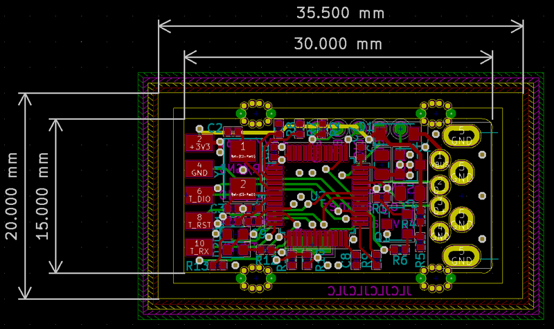
For SMT assembly, JLCPCB has a minimum size of 20 mm in either direction:
For a USB stick 20 mm is too wide, so I had to design the PCB with a breakaway part connected with mouse bites.
The final rev. a layout looks like this:
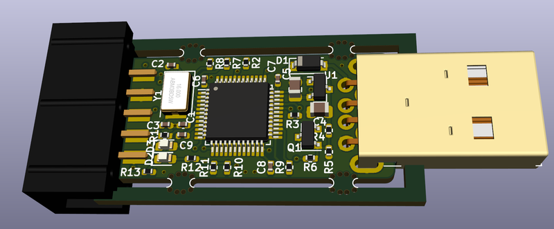
The KiCAD 3D model:
Revision a
A quick order to JLCPCB and within a week I had my first "samples".
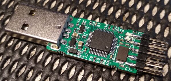
I had to solder the USB connector by hand and it turned out that I was either out of IDC connectors (or couldn't be bothered to search long enough to dig them out of a box), so I used a simple dual-row standard 100 mil header.
That is "good enough". For rev. b, I will put 1 mm more spacing between the IDC header and the components - that was a bit tight.
Firmware
To be added
Testing
To be added
