Difference between revisions of "STM32 Internal Flash Layout"
Jump to navigation
Jump to search
| (4 intermediate revisions by the same user not shown) | |||
| Line 13: | Line 13: | ||
[[File:STM32F103xx Flash Page Layout.png|600px]] | [[File:STM32F103xx Flash Page Layout.png|600px]] | ||
| + | |||
| + | == STM32L0x2 and STM32L0x3 == | ||
| + | From [https://www.st.com/resource/en/reference_manual/rm0376-ultralowpower-stm32l0x2-advanced-armbased-32bit-mcus-stmicroelectronics.pdf Reference Manual] and [https://www.st.com/resource/en/reference_manual/DM00095744-.pdf Reference Manual] | ||
| + | |||
| + | [[File:STM32L0x2 Flash Page Layout.png|600px]] | ||
== STM32L151 == | == STM32L151 == | ||
Latest revision as of 08:49, 24 June 2023
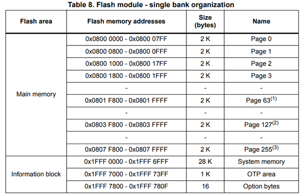
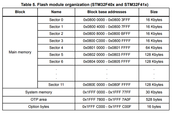
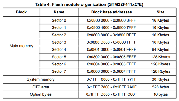
One confusing aspect of STM32 is that the flash layout differ greatly between families and even individual MCUs within a family. On some families flash can be erased by page - typically 1 KB or 2 KB. On others erase can only be done per sector and the sectors are not of the same size. The information is in the reference manual of each MCU.
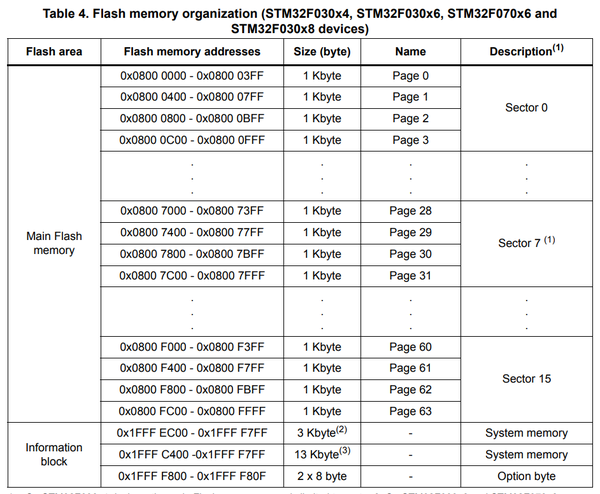
STM32F030
From Reference Manual
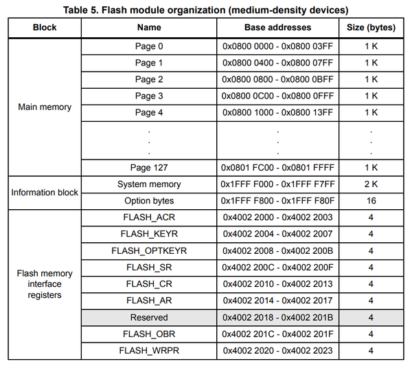
STM32F103
From Reference Manual
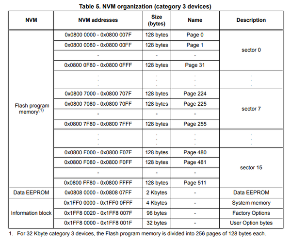
STM32L0x2 and STM32L0x3
From Reference Manual and Reference Manual
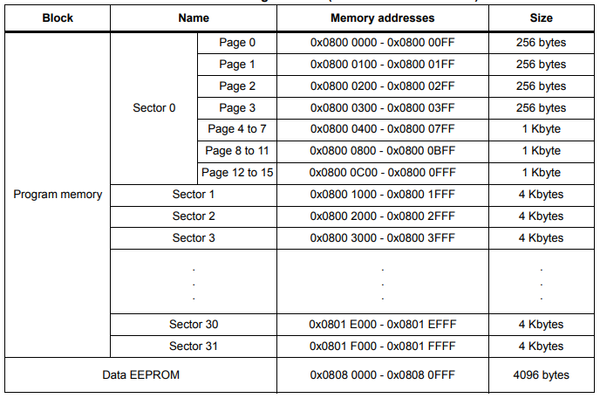
STM32L151
From Reference Manual
STM32L432
From Reference Manual
STM32F405
From Reference Manual
STM32F411
From Reference Manual:
