Difference between revisions of "Stm32Dev - rev. b"
| (3 intermediate revisions by the same user not shown) | |||
| Line 1: | Line 1: | ||
| − | [[Category:STM32]][[Category:STM32 Development Board]][[Category:STM32F405]][[Category:STM32 Hardware Development]]{{metadesc|Own design STM32 development board | + | [[Category:STM32]][[Category:STM32 Hardware]][[Category:Development Board]][[Category:STM32 Development Board]][[Category:STM32F405]][[Category:STM32 Hardware Development]]{{metadesc|Own design STM32 development board}} |
[[File:Stm32Dev rev. b - top side unpopulated.jpg|thumb|STM32Dev rev. b]] | [[File:Stm32Dev rev. b - top side unpopulated.jpg|thumb|STM32Dev rev. b]] | ||
When designing the [[Stm32Dev - first version]] a number of mistakes was made. This lead naturally to the development of [[Stm32Dev - rev. b]]. | When designing the [[Stm32Dev - first version]] a number of mistakes was made. This lead naturally to the development of [[Stm32Dev - rev. b]]. | ||
| + | |||
| + | While the overall design is identical to the first version, a number of tweaks were made. These include: | ||
| + | |||
| + | * Double headers | ||
| + | * Different choice of [[LDO]] | ||
| + | * Buttons for [[NRST]] and [[Boot0]] | ||
| + | * 8 MHz Crystal | ||
| + | * Regular blue [[LED]] on PC13 | ||
| + | * [[WS2812B]] hanging off of PC6 | ||
| + | * SD-Card | ||
| + | |||
| + | The reasoning behind these choices should be pretty darn obvious, but let me go through them anyway. | ||
| + | |||
| + | [[File:Jumper leads on headers.jpg|thumb|Jumper leads on headers]]I absolutely positively despise breadboards. True, I might have had bad experiences because my breadboards were cheap crap, but I find myself spending more time chasing down lose connections than I do doing anything productive, so I generally much prefer just to wire stuff up using jumper leads directly on the headers. By using that approach I regularly end up in a situation where I need two leads connected to one pin, hence having a dual row is convenient. | ||
| + | |||
| + | The [[LDO]] on the original board was massively over dimensioned (can handle up to 1-2 amps). Switched that to a [https://lcsc.com/product-detail/Dropout-Regulators-LDO_Torex-Semicon-XC6206P332MR_C5446.html Torex Semicon XC6206P332MR] which will happily handle the 500 mA possible from a [[USB]] port. | ||
| + | |||
| + | Having the buttons is just a massive convenience on a development board. | ||
| + | |||
| + | The Micro-SD was added as an afterthought. There was space available and footprints are free. Since I had used it in a previous project and had a few lying around, I used the [https://lcsc.com/product-detail/Card-Sockets-Connectors_HRS-Hirose-DM3D-SF_C719027.html Hirose DM3D-SF] connector. | ||
| + | |||
| + | == Schematics == | ||
| + | |||
| + | The full schematics is as: | ||
| + | |||
| + | [[File:Stm32dev rev. b.svg|1000px]] | ||
| + | |||
| + | As [[LDO]] regulator we are using the [https://www.torexsemi.com/file/xc6206/XC6206.pdf Torex XC6206]. It will quite happily handle around 200 mA (actually more) which is more than enough to drive a [[STM32]] and a few peripherals. The regulator is decoupled on each side with a 10 uF capacitor, which is the maximum value according to the USB specification (to prevent high inrush current which could shut down the USB port). | ||
| + | |||
| + | Two buttons are used for the [[NRST]] and [[Boot0]] pins. According to the [https://ipfs.subutai.io/ipfs/QmSFtdDUKXV7Fwd7pz4g3Qn8vM1e1kHENAxgvptZQYvmBC/DM00037051.pdf STM32F405 datasheet], the NRST is pulled up internally, so the NRST pull-up resistor is not mounted. Likewise, the Boot0 pin needs to be pulled high forcefully to trigger the bootloader, so the external pull-down on that is not mounted. | ||
| + | |||
| + | Two regular [[LED]]s are mounted on the board. One connected straight to the +3.3 V rail, and one to the PC13 GPIO pin. The use of PC13 is mainly because that seems to be a bit of a standard on development boards. The pin as such is not ideal for driving a LED as it can NOT do pulse-width modulation ([[PWM]] - see [[STM32 LED Blink]]). The choice of 1K current limiting resistors result in a fairly weak brightness (but very low current consumption). | ||
| + | |||
| + | A second RGB LED ([[WS2812B]]) is attached to PC6. | ||
| + | |||
| + | == Production Files == | ||
| + | |||
| + | The production files are available [https://github.com/lbthomsen/stm32dev/tree/master/pcb here]. The gerber files are in stm32dev_b.zip and the bom and placement files are in stm32dev_b_bom.csv and stm32dev_b_pos.csv. | ||
== PCB == | == PCB == | ||
| Line 9: | Line 47: | ||
{| | {| | ||
|- | |- | ||
| − | |[[File:Stm32Dev rev. b - top side unpopulated.jpg| | + | |[[File:Stm32Dev rev. b - top side unpopulated.jpg|500px]] |
| − | |[[File:Stm32Dev rev. b - unpopulated.jpg| | + | |[[File:Stm32Dev rev. b - unpopulated.jpg|500px]] |
|} | |} | ||
The USB-C connector, the SD, the ws2812 and all the headers have not been mounted by jlcpcb. | The USB-C connector, the SD, the ws2812 and all the headers have not been mounted by jlcpcb. | ||
Latest revision as of 02:40, 28 October 2021
When designing the Stm32Dev - first version a number of mistakes was made. This lead naturally to the development of Stm32Dev - rev. b.
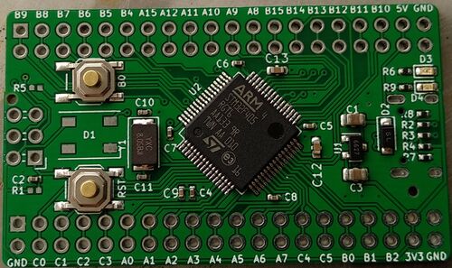
While the overall design is identical to the first version, a number of tweaks were made. These include:
- Double headers
- Different choice of LDO
- Buttons for NRST and Boot0
- 8 MHz Crystal
- Regular blue LED on PC13
- WS2812B hanging off of PC6
- SD-Card
The reasoning behind these choices should be pretty darn obvious, but let me go through them anyway.
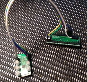
I absolutely positively despise breadboards. True, I might have had bad experiences because my breadboards were cheap crap, but I find myself spending more time chasing down lose connections than I do doing anything productive, so I generally much prefer just to wire stuff up using jumper leads directly on the headers. By using that approach I regularly end up in a situation where I need two leads connected to one pin, hence having a dual row is convenient.
The LDO on the original board was massively over dimensioned (can handle up to 1-2 amps). Switched that to a Torex Semicon XC6206P332MR which will happily handle the 500 mA possible from a USB port.
Having the buttons is just a massive convenience on a development board.
The Micro-SD was added as an afterthought. There was space available and footprints are free. Since I had used it in a previous project and had a few lying around, I used the Hirose DM3D-SF connector.
Schematics
The full schematics is as:
As LDO regulator we are using the Torex XC6206. It will quite happily handle around 200 mA (actually more) which is more than enough to drive a STM32 and a few peripherals. The regulator is decoupled on each side with a 10 uF capacitor, which is the maximum value according to the USB specification (to prevent high inrush current which could shut down the USB port).
Two buttons are used for the NRST and Boot0 pins. According to the STM32F405 datasheet, the NRST is pulled up internally, so the NRST pull-up resistor is not mounted. Likewise, the Boot0 pin needs to be pulled high forcefully to trigger the bootloader, so the external pull-down on that is not mounted.
Two regular LEDs are mounted on the board. One connected straight to the +3.3 V rail, and one to the PC13 GPIO pin. The use of PC13 is mainly because that seems to be a bit of a standard on development boards. The pin as such is not ideal for driving a LED as it can NOT do pulse-width modulation (PWM - see STM32 LED Blink). The choice of 1K current limiting resistors result in a fairly weak brightness (but very low current consumption).
A second RGB LED (WS2812B) is attached to PC6.
Production Files
The production files are available here. The gerber files are in stm32dev_b.zip and the bom and placement files are in stm32dev_b_bom.csv and stm32dev_b_pos.csv.
PCB
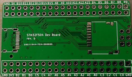
Based on the above production files, a run of 5 boards were ordered at JLCPCB. They were received like this (and yes - we are aware of the silkscreen typo):

|

|
The USB-C connector, the SD, the ws2812 and all the headers have not been mounted by jlcpcb.


