Difference between revisions of "Stm32Dev - rev. b"

From Stm32World Wiki
Jump to navigation Jump to search
Line 1: Line 1:
[[Category:STM32]][[Category:STM32 Development Board]][[Category:STM32F405]][[Category:STM32 Hardware Development]]{{metadesc|Own design STM32 development board}}
+
[[Category:STM32]][[Category:STM32 Development Board]][[Category:STM32F405]][[Category:STM32 Hardware Development]]{{metadesc|Own design STM32 development board with gd32f405 mcu}}
 
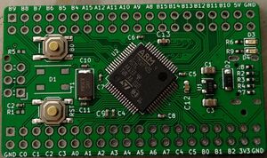
[[File:Stm32Dev rev. b - top side unpopulated.jpg|thumb|STM32Dev rev. b]]
 
[[File:Stm32Dev rev. b - top side unpopulated.jpg|thumb|STM32Dev rev. b]]
 
When designing the [[Stm32Dev - first version]] a number of mistakes was made.  This lead naturally to the development of [[Stm32Dev - rev. b]].
 
When designing the [[Stm32Dev - first version]] a number of mistakes was made.  This lead naturally to the development of [[Stm32Dev - rev. b]].
 
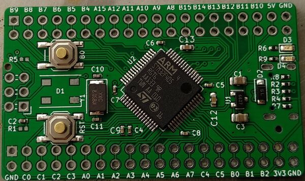
While the overall design is identical to the first version, a number of tweaks were made.  These include:
 
 
* Double headers
 
* Different choice of [[LDO]]
 
* Buttons for [[NRST]] and [[Boot0]]
 
* 8 MHz Crystal
 
* Regular blue [[LED]] on PC13
 
* [[WS2812B]] hanging off of PC6
 
* SD-Card
 
 
The reasoning behind these choices should be pretty darn obvious, but let me go through them anyway.
 
 
[[File:Jumper leads on headers.jpg|thumb|Jumper leads on headers]]I absolutely positively despise breadboards.  True, I might have had bad experiences because my breadboards were cheap crap, but I find myself spending more time chasing down lose connections than I do doing anything productive, so I generally much prefer just to wire stuff up using jumper leads directly on the headers.  By using that approach I regularly end up in a situation where I need two leads connected to one pin, hence having a dual row is convenient.
 
 
The [[LDO]] on the original board was massively over dimensioned (can handle up to 1-2 amps).  Switched that to a [https://lcsc.com/product-detail/Dropout-Regulators-LDO_Torex-Semicon-XC6206P332MR_C5446.html Torex Semicon XC6206P332MR] which will happily handle the 500 mA possible from a [[USB]] port.
 
 
Having the buttons is just a massive convenience on a development board.
 
 
The Micro-SD was added as an afterthought.  There was space available and footprints are free.  Since I had used it in a previous project and had a few lying around, I used the [https://lcsc.com/product-detail/Card-Sockets-Connectors_HRS-Hirose-DM3D-SF_C719027.html Hirose DM3D-SF] connector.
 
 
== Schematics ==
 
 
The full schematics is as:
 
 
[[File:Stm32dev rev. b.svg|1000px]]
 
 
As [[LDO]] regulator we are using the [https://www.torexsemi.com/file/xc6206/XC6206.pdf Torex XC6206].  It will quite happily handle around 200 mA (actually more) which is more than enough to drive a [[STM32]] and a few peripherals.  The regulator is decoupled on each side with a 10 uF capacitor, which is the maximum value according to the USB specification (to prevent high inrush current which could shut down the USB port).
 
 
Two buttons are used for the [[NRST]] and [[Boot0]] pins.  According to the [https://ipfs.subutai.io/ipfs/QmSFtdDUKXV7Fwd7pz4g3Qn8vM1e1kHENAxgvptZQYvmBC/DM00037051.pdf STM32F405 datasheet], the NRST is pulled up internally, so the NRST pull-up resistor is not mounted.  Likewise, the Boot0 pin needs to be pulled high forcefully to trigger the bootloader, so the external pull-down on that is not mounted.
 
 
Two regular [[LED]]s are mounted on the board.  One connected straight to the +3.3 V rail, and one to the PC13 GPIO pin.  The use of PC13 is mainly because that seems to be a bit of a standard on development boards.  The pin as such is not ideal for driving a LED as it can NOT do pulse-width modulation ([[PWM]] - see [[STM32 LED Blink]]).  The choice of 1K current limiting resistors result in a fairly weak brightness (but very low current consumption).
 
 
A second RGB LED ([[WS2812B]]) is attached to PC6.
 
 
== Production Files ==
 
 
The production files are available [https://github.com/lbthomsen/stm32dev/tree/master/pcb here].  The gerber files are in stm32dev_b.zip and the bom and placement files are in stm32dev_b_bom.csv and stm32dev_b_pos.csv.


== PCB ==  
 
== PCB ==  

Revision as of 03:49, 11 May 2021

STM32Dev rev. b

When designing the Stm32Dev - first version a number of mistakes was made. This lead naturally to the development of Stm32Dev - rev. b.

PCB

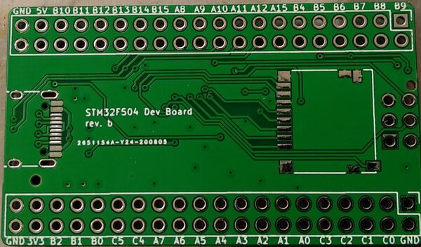
Based on the above production files, a run of 5 boards were ordered at JLCPCB. They were received like this (and yes - we are aware of the silkscreen typo):
Stm32Dev rev. b - top side unpopulated.jpg Stm32Dev rev. b - unpopulated.jpg

The USB-C connector, the SD, the ws2812 and all the headers have not been mounted by jlcpcb.